Subproject A3
Thin film technologies for metal-based piezoelectric modules
Project Managers:
Prof. Dr. rer. nat. habil. Frank RichterChemnitz University of Technology
Institute of Physics
Reichenhainer Str. 70
09107 Chemnitz
Telephon: +49-(0)371 / 531 38046
Telefax: +49-(0)371 / 531 21719
E-Mail: f.richter@physik.tu-chemnitz.de
Dr. rer. nat. Siegfried Peter
Chemnitz University of Technology
Institute of Physics
Reichenhainer Str. 70
09107 Chemnitz
Telephon: +49-(0)371 / 531 38258
Telefax: +49-(0)371 / 531 838258
E-Mail: s.peter@physik.tu-chemnitz.de
Presenting the Research Program
Program and results of the first research period
| This subproject pursued the aim of producing and optimizing an insulation layer integrated in the metal-based piezoelectric module (Figure 1) within the PIESA-process chain “sheet metal”. The main focus laid on the deposition of electrical and mechanical highly resilient thin layers on micro-structured lightweight metal plates (sheet metal). To keep the thermal load on the lightweight structures low, the insulation layers were produced by means of low temperature, plasma enhanced chemical vapour deposition (PECVD). | 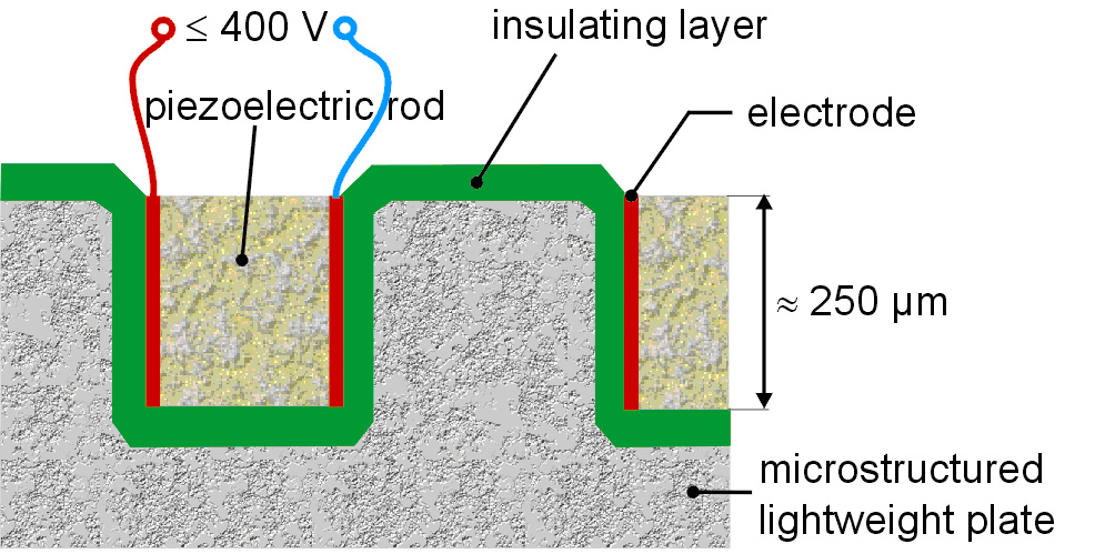 |
|
| Fig. 1: Metal-based piezoelectric module |
Besides the requirements concerning the Young’s modulus (? Young’s modulus of lightweight metal) and the electrical characteristics of high di-electric strength and low leakage current, the uniform coverage of the microcavities had made it necessary to further develop the coating material (Figure 2) and the PECVD process (Figure 3).
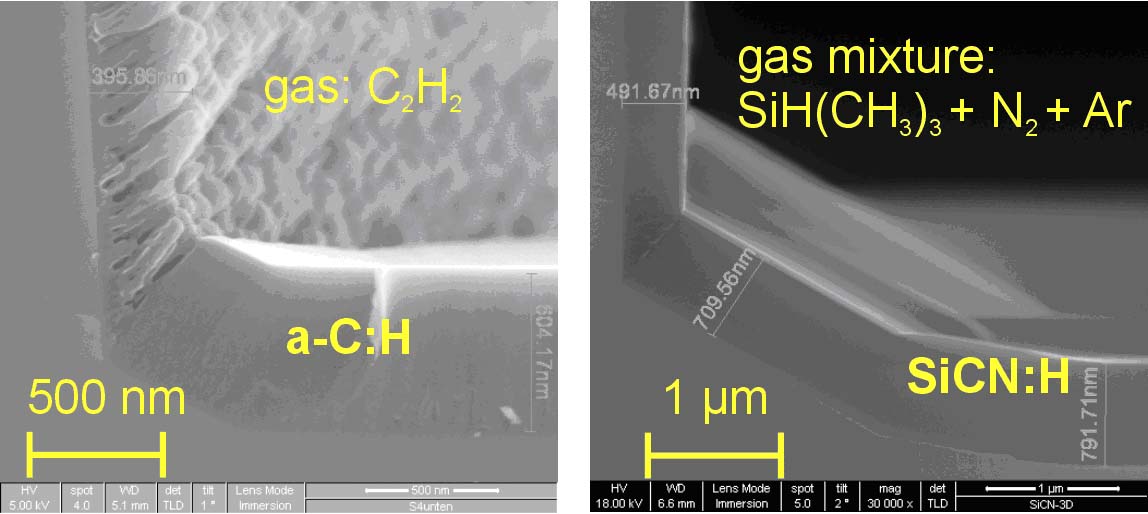 |
Fig. 2: Improvement of film morphology inside microcavities by changing from amorphous hydrogenated carbon films (a-C:H) to amorphous hydrogenated silicon carbonitride films (a-SiCN:H) (cross fractures of coated microstructures; SEM views at lower edges) |
|
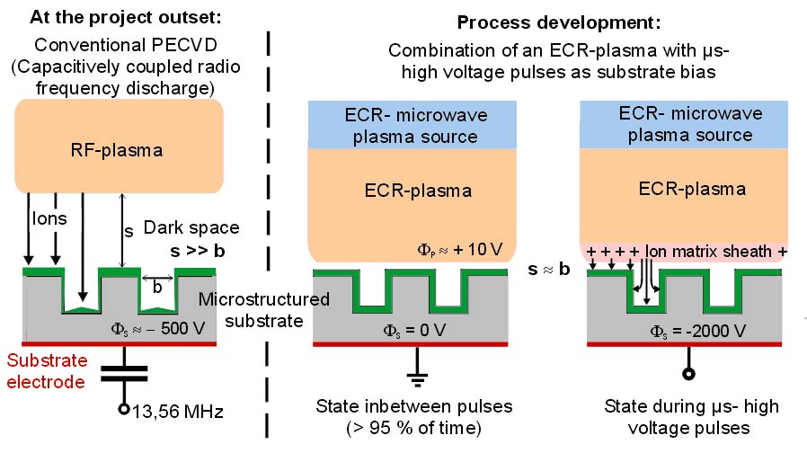 |
Fig. 3: Pictorial schematic of film profiles (green) evolved during deposition from capacitively coupled radio frequency discharges (left) and from electron cyclotron resonance (ECR) microwave plasmas with µs-pulsed substrate bias (right) |
Second Research Period - Motivation
In this period, the main focus is to assure the functionality of the insulating layer on piezoelectric fibres-epoxy composites (manufactured in sub-project A1), which are temperature-sensitive. As found in period 1, the insulation layers for the lightweight metal-based piezoelectric modules have to be electrical and mechanical highly resilient. Besides the applied voltages up to 400 V, it is also necessary that small strains (less than 250 nm) occurring for the piezoelectric bars are transferred nearly without any losses to the microstructured lightweight metal. This means that Young’s modulus of the coatings has to be about 80 GPa or more. Thus, the insulation layers have to meet similar requirements concerning their mechanical characteristics. Moreover, to assure their functionality, the layers have to comply with certain loading conditions during subsequent process steps, such as bonding, forming and joining. One advantage of the new concept is to replace the vacuum deposition process on the micro-structured light-weight metal plates.
| Figure 4 shows an SEM image of the cross-section of a lead zirconate titanate (PZT) covered by a thin gold layer as electrode (commercial product). This figure draws attention to the challenge of depositing layers on PZT. The gold layer is poorly adhered to the PZT grains, is rich of defects and with a Young’s modulus of nearly 20 GPa mechanically much less stiffer than bulk gold (Young’s modulus of 70 GPa). Therefore he deposition of those insulating layers in the case of temperature-sensitive piezoelectric fibres-epoxy composites is highly challenging, thus being the main focus of the second period. | 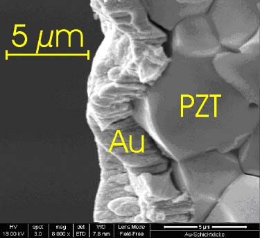 |
Fig. 4: SEM image of a PZT plate covered by a thin gold electrode layer. |
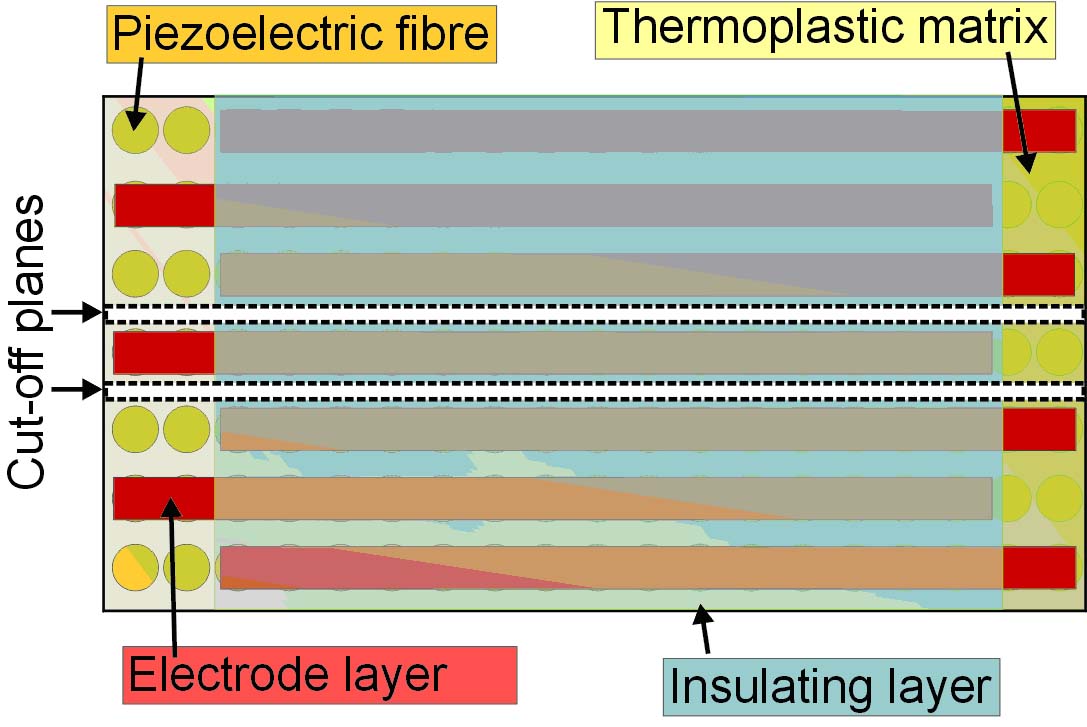 |
Fig. 5:
Electrode and insulation layers deposited on piezo-electric fibres–epoxy composites used for manufacturing of ladder-like structures of piezoelectric composites (project area A).
|
For effective mounting processes (subproject A2) as well as for bonding (A4, A6), it is desired that both the electrode and the insulation layers are structured (Fig. 5). Since the piezoelectric fibres - epoxy composites are very inhomogeneous substrates for the deposition of metallic and insulating layers, the requirements are to be meet only by a detailed consideration of each individual material and interface in the given system (i.e. piezoelectric material and electrode materials, insulation layer, lightweight metal). |
Approach
 |
To reduce the thermal load to the piezoelectric fibres - epoxy composites during deposition, the temperature should be less than 150 °C. Magnetron sputtering has been chosen for the deposition of the metallic electrode layer, while the insulation layers (a-SiCN:H) as well as, if necessary, interlayers for improving adhesion are produced by means of PECVD (Fig. 6).
One main research objective in this framework is the investigation of the problem of adhesion as well as the development of thermal and mechanical stresses during deposition and during the subsequent manufacturing process steps.
Secondly, the research work focuses on the investigation of basic mechanisms of thin film growth on insulating substrates, such as PZT or epoxy. The final goal is to better understand the interdependence of deposition and plasma parameters, film structure and film properties.
Since the realization of the deposition of electrical and mechanical highly resilient layers necessitates a film growth under ion bombardment, which is not a trivial task for insulating substrates, suitable methods for plasma generation and controlling ion bombardment are to be found. On the other hand, techniques for measurement of particle flux (electrons, ions) to the substrate and their energy as well as resulting thermal load are to be devel-oped. For instance, to measure the temperature of the substrate surface during deposition, a two colour pyrometer is to be adapted.
|
|
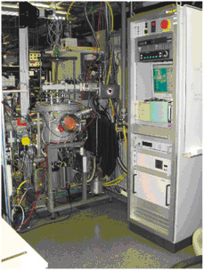
| Fig. 6: Deposition system MicroSys400 (Roth&Rau) used for magnetron sputtering and PECVD. |